Technology for the Accurate Preparation of Silicon Capacitive Pressure Sensors with Biomedical Application
Introduction
The basic technology to achieve capacitive sensors for biomedical applications is related to the silicon planar processing [1,2], showing the evident advantage of the possibility to prepare numerous devices (of the order of thousand) on the same silicon wafer during the same series of successive processes, and of the high experience accumulated in the fabrication of the microelectronic intelligent chips of microprocessors and microelectromechanical systems (MEMS). As a consequence, a remarkable growth and diversification of such devices have been developed in an accelerated rhythm, especially in the last four decades, including the achievement of the silicon-based sensors for biomedical applications [3], like: silicon MEMS-type microphone for the determination of the pulse, silicon nanowires for the detection of deoxyribonucleic acid (DNA) molecules, silicon probe-polyimide monolithic sensor systems for the detection of the neural activity, silicon-based CMOS (complementary metaloxide- semiconductor) and BiCMOS (combined bipolar junction transistor and the CMOS gate) for the detection of the heartbeat, respiration and of the peripheral and cranial nerve activities, silicon-silicon-dioxide-chromium for the detection of the proteins and photo lipids, nitrogen-doped silicon to detect specific proteins, amorphous silicon-image sensor based on thin-film transistors for X-ray medical imaging.
The spectrum of capacitive pressure sensor application is also increasing in the last decade [4] including MEMS materials used in fabrication, procedures adopted in microfabrication for silicon and polymer material diaphragm, and bonding and the used packaging techniques. Even so, no correlation between diffusion profile and etching rate was reported up to date within the frame of the bulk micromachining technology, although this is a key requirement for an accurate control of the MEMS sensitive elements, particularly of the silicon membranes of the capacitive sensors for biomedical applications, so this problem is approached here, referring specifically to the preparation of the capacitive silicon sensors to measure the blood pressure. These miniature sensors (with area of the order of a few millimeters and the membrane diameter of the order of 100 micrometers) [5-7] can be implanted in the human body and can be monitored telemetrically without wires breaking the skin [8]. These sensors can provide a dynamic range of 0-50 mmHg over atmospheric pressure and their sensitivity response can be calculated as a function of their geometrical and material characteristics [9,10].
The control of the sensor geometry and material characteristics during the technological processes of fabrication is a prime engineering task. Based on the specific properties of boron layers to decrease the chemical etching rate [11,12], the boron diffusion in silicon became a largely used technique for the fabrication of the micro-mechanical structures within the bulk micromachining technology [4,13], particularly the silicon membranes for pressure sensor application. This is based on the self-limitation of the etching process at high boron concentration, assumed to be uniform. However, the boron concentration is variable, decreasing from the silicon surface to the bulk, according to the diffusion law, so a correct preparation of the membrane thickness can be obtained only if the boron diffusion profile can be adequately controlled. Therefore, this paper presents an accurate method to control the technological process of the boron diffusion and of the subsequent etching process for the membrane achievement of the capacitive silicon capacitive sensors for biomedical applications, by solving the non-linear diffusion equation in the range of high concentration, on which the diffusion coefficient depends on the square root of the boron concentration, during the diffusion from oxidation-assisted boron tribromide (BBr3) liquid and (B2O3) local deposited sources.
The analytical solution obtained on this way allows to calculate the boron diffusion profile, the chemical etching rate and finally the etching time, necessary to stop the etching process in an adequate moment, so that the entire preparation process can be correctly designed and controlled on the fabrication line, as it is presented below.
Calculation of the Boron Diffusion Profiles in Silicon for the Preparation of the Highly Doped Stop Layers
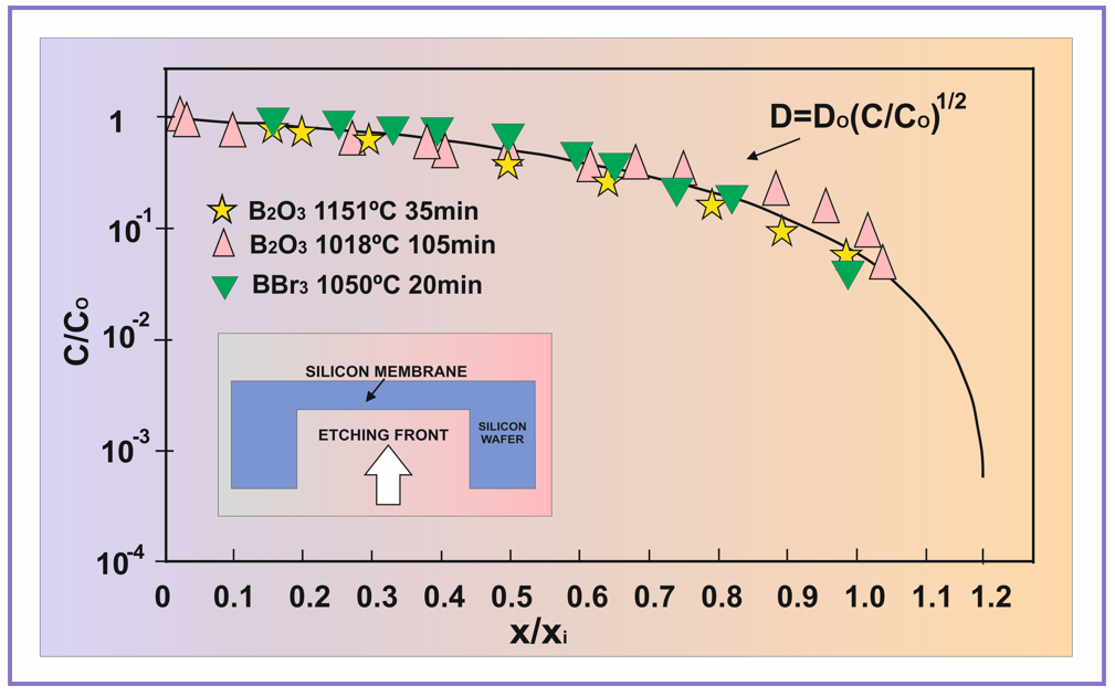
The boron diffusion profile consists in the distribution of the boron concentration in the silicon bulk during and after the diffusion, which decreases gradually from the silicon surface (in this case in permanent contact with the diffusion source) to the depth into the silicon bulk. A schematic representation of the technological process to obtain the silicon capacitive pressure sensors is shown in the inserted drawing in the left side of the (Figure 1). Silicon wafers are lithographically processed to allow the local diffusion of boron and the chemical etching process [12], which advances from the back side to the highly-boron-doped layer, where the chemical rate begins to decrease progressively, depending on the boron concentration. There are two ranges of interest in the boron diffusion profile at high concentrations: the intrinsic range, where the boron concentration C is lower than the intrinsic carrier concentration ni at the diffusion temperature [1,2,14], and the extrinsic range, where C>ni. The intrinsic carrier concentration (ni) depends on temperature too, but its variation is very slow, around 1019cm-3 [14] for the usual diffusion within the interval 1050°C–1200°C, i.e. with a variation between 9×1018cm-3 and 1.8×1019cm-3 respectively.
In the high concentration range, the boron concentration is a function of the diffusion depth, so the etching process depends on the variation of the boron concentration in the bulk. The main problem concerning the achievement of silicon membranes with certain well-defined thickness according to the design requirements and the sensitivity range of the pressure, is therefore strictly related to the control of the technological process. Such a control requires a practical method to calculate the boron diffusion profile in silicon, according to the technological used parameters, time and temperature and also to the type of the diffusion source. Diffusion is therefore a key process to control the parameters of the capacitive sensors. In (Figure 1) are represented experimental data determined after boron diffusion at high concentration under oxidation conditions (BBr3 with oxygen in the diffusion furnace tube or B2O3 local deposited source on the silicon wafers surface), normalized to the surface concentration Co vs. normalized depth x / xi into the silicon bulk, where x is the depth and xi is a value corresponding to the intrinsic carrier concentration, which delimits the diffusion range where the diffusion coefficient does really depend on concentration [15,16].
Figure 1: Normalized boron diffusion profiles C / Co vs. x / xi experimentally determined after diffusion at 1151°C and 1018°C for 35 and 105 min. respectively from B2O3 source (data collected from ref. [19]), and BBr3 source at 1050°C for 20 min. (data collected from ref. [20]), determined by an electrical method, compared with the normalized (universal) profile, theoretically deduced in this paper as a solution of the non-linear diffusion equation for  .
.
The analysis of the diffusion profiles represented under this form in (Figure 1) shows that these profiles obey a universal curve, independent on diffusion time and temperature, characteristic for a dependence of the diffusion coefficient D on concentration as  , where Do = D(x = 0) . This finding allows to approach the solving of the boron diffusion problem in silicon along the x direction into the silicon bulk from a diffusion source in permanent contact with the silicon surface, expressible by a partial differential equation with the variables x and t (diffusion time), of the form:

This is not an easy problem [16-18], but a solution can be searched by using a series technique, which leads in this case to an analytical solution of the simple form:

where  , expressed as the diffusion depth x, normalized to the diffusion length
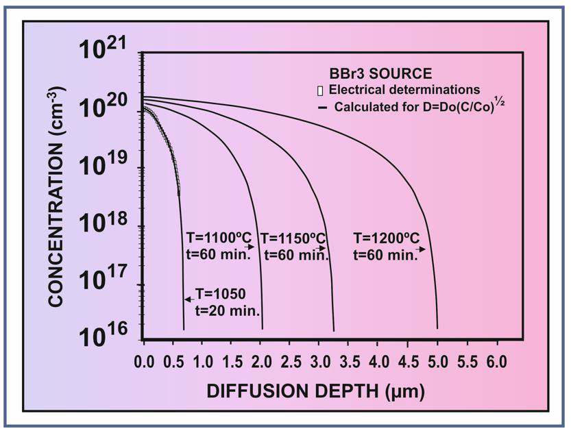
This is an approximate solution of the diffusion equation, but with an approximation error less than 1%. As it can be seen from (Figure 1), the agreement between the calculated profile (solid line in (Figure 1) and experimental data collected from [19, 20] is very good. In (Figure 2) are shown calculated boron diffusion profiles after diffusion from BBr3 source at sufficiently high temperatures (1050°C, 1100°C, 1150°C and 1200°C), useful for the preparation of the silicon capacitive pressure sensors with various membrane thicknesses, in the range of 0.4 – 4.0 micrometers, and a comparison of the theoretical profile with experimental data after diffusion from BBr3 source of 20 min. at 1050°C collected from [20], showing a very good agreement. On the extrinsic concentration range (C>ni), the entire quantity of boron atoms is ionized, so that the concentration of the electrical carriers is the same with boron concentration, as it was previously demonstrated [18].
A remarkable property of this solution is that the concentration becomes zero for a finite value  . Such a property is a consequence of the specific dependence of D on concentration C (in this case on C1/2), which makes the diffusion flux all the smaller as the concentration decreases, eventually becoming zero [15]. In the real situations however, the diffusion process continues in the lower concentration (intrinsic) range with a constant diffusion coefficient, but this domain is not relevant from the point of view of the etching process, because the etching rate is not inhibited practically by boron concentration lower than a critical value Cc (C>ni), specific for the etching process, as it will be shown below.
Figure 2: Calculated profile from BBr3 source (solid line) compared with experimental data of diffusion at 1050°C for 20 min. collected from ref. [20], and calculated boron diffusion profiles after 60 min. diffusion at 1100°C, 1150°C, 1200°C (solid lines), suitable for the capacitive pressure sensor preparation.
Calculation of the Chemical Etching Rate and Etching Time for the Membrane Achievement
The alkaline type solutions KOH, NaOH, LiOH or EDP (ethylenediamine- pyrocatechol) are effective selective etching chemical agents for the achievement of thin silicon membranes [21], with a specific dependence of the etching rate R on the type of solution, the temperature Tc of the etching process and on the boron concentration C in silicon, as follows:

where Ri represents the etching rate of the low-doped (intrinsic) silicon substrate, Cc is a critical value in the range (2- 4)×1019 cm-3, which depends on the etching temperature Te and on the concentration of the etching solution of the alkaline type (KOH, NaOH, LiOH) or of EDP, and “a” is a shape parameter: a=4 corresponds to 10% KOH (NaOH, LiOH) and ethylene-diaminebased (EDP) solution, and a=2 to 24% alkaline-type solutions [21]. However, in the above relation, the silicon layers are considered to be uniformly doped with a constant concentration C, which do not really correspond to reality. Therefore, for an effective and accurate control of the etching process for the membrane achievement of the silicon capacitive pressure sensors, it is necessary to dispose of an explicit relation between the etching rate R and the boron diffusion depth in silicon. The relation expressing the dependence of the etching rate R on the silicon depth x can be obtained by introducing the boron doping concentration C (rel.(2)) found above as a solution of the diffusion equation, into rel. (3).
Furthermore, taking into account that the etching front advances to the silicon doped surface along the diffusion direction, but in the contrary sense with a rate R = dx / dt [22], the chemical etching time t necessary to etch a boron diffusion layer can be deduced as following:

and can be finally calculated as:

where xi is the depth limit of the intrinsic domain, Δt = t − to (to – the initial moment at xi boundary), and τ is defined as τ = xi / Ri . For an adequate control of the etching process given by the relations (3) and (5), the values Cc for various reaction temperatures Tc should be known. This dependence was obtained by a best fitting procedure of the Cc experimental data as a function of the temperature Tc previously reported [21], so that the following expression was obtained:

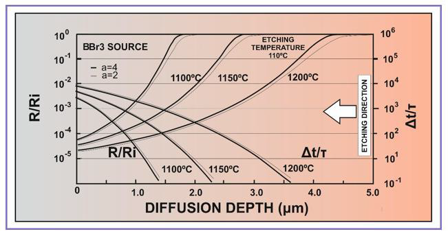
where k is the Boltzmann constant. As Ce in rel. (3) defines a critical values of the boron concentration (usually in the range (2-4) ×1019 cm-3), for which the etching rate R begins to decrease significantly, the variation of R in the intrinsic range (C< ni < Cc) is actually negligible, as it was mentioned above. In (Figure 3) is shown the variation of the ratio R/Ri with the depth x into the silicon boron-doped layer after diffusions at 1100oC, 1150oC and 1200oC by using alkaline type (KOH, NaOH, LiOH) or of EDP solutions at 110°C for which a = 4 and a=2, and the corresponding variation of the necessary etching time. From (Figure 3) it can be observed a slower variation of the etching process in a solution corresponding to a=2, but both types of solutions (a=2 and a=4) are efficient for the silicon membrane preparation, showing values of about 103 times higher near silicon surface than the values corresponding to Ri in the low-doped (intrinsic) silicon bulk. The increase of the diffusion temperature allows to obtain larger values of the membrane thickness for the same etching duration, and determines an increase of the etching duration, if the same value of the membrane thickness is required.
Figure 3: The calculated R / Ri ratio and  during the chemical etching process of the boron silicon layers diffused from BBr3 source at 1100°C, 1150°C and 1200°C for 60 min, in etching solutions with a=2 and a=4 at 110°C.
Taking into account the fine differences exhibited in (Figure 3). a fine tuning of the boron diffusion conditions and of the etching process should be applied not only to sharply define the thickness of the silicon membranes, but also for the elimination of the diffused regions where the concentration gradient is sufficiently large to induce mechanical stress into the silicon membrane, creating undesired curvatures of the membranes and therefore their incorrect response to the applied pressure. As it can be observed from (Figure 2), the higher diffusion time, the lower diffusion gradient is obtained in the highly doped region. The obtained results presented above allow a suitable management for the accurate control and optimization of the appropriate technological parameters, serving also as predicting data for the design of the silicon membranes for the preparation of the capacitive silicon pressure sensors for biomedical applications.
Conclusion
It was highlighted the key importance of the boron diffusion process for the accurate preparation of the membranes of the capacitive pressure sensors for biomedical applications, so a main objective of this investigation was to deduce the variation of the boron diffusion coefficient with the boron concentration and the corresponding solution of the boron diffusion equation on the high concentration range, where the boron doped layers can serve as stop layers for the etching process. From the analysis of the experimental data after diffusion from oxidation-assisted sources (BBr3 and B2O3), it was deduced a dependence of the boron diffusion coefficient on the boron concentration of the form  , and it was obtained an analytical solution of the partial differential non-linear diffusion equation, showing a very good agreement with the experimental data on the high concentration range. This solution was used for further calculation of the chemical etching rate and etching time for the preparation under various process conditions of the sensing membrane for the achievement of the silicon capacitive sensors with biomedical applications.
The derived expression for the calculation of the chemical etching rate and the etching time allows an appropriate and fine-tuning control of the etching process as a function of the variation of the boron diffusion concentration with the silicon depth after diffusion at various temperatures and time duration, demonstrating the high applicability of the analytical results in a large range of variation of the technological parameters, serving both for the suitable management of the chemical etching process and the device design of the capacitive silicon pressure sensors. The presented results allow also an accurate control of the doped layer regions of high concentration gradient inducing residual stress and their elimination, to avoid undesirable deformations of the silicon membranes.
For more Articles on: https://biomedres01.blogspot.com/


No comments:
Post a Comment
Note: Only a member of this blog may post a comment.