The topic of silicon nanowires (Si-NWs) is a timely emergent study. Over the last few years Si-NWs have come under intensive research as a result of their potential characteristics and conceivable as key materials in advanced optoelectronic applications [1-3]. The review work on a fast-developing topic is not a trivial objective, and it is even more critical with nanotechnology-related subject matters. This review is focused on experimental work and progress of silicon nanowires (Si-NWs) technology for the past decades, with more focus on the last decade work. Si-NWs are particularly important, based on the well-known fact of the technological importance of Si material. Moreover, the particular advantages of nano-morphology of high ratio of the area of the surface to the corresponding volume and their related applications [4]. Any application take place at the outer sur-face of the material such as chemical reactions or photon absorption, it will obviously speed up at that surface of extremely high area [4,5]. Indeed, there are potential features of Si-NWs to be integrated with the available applications, such as, photovoltaic (PV) [2,4,6]. The transistor of Metal Oxide Semiconductor Field Effect would benefit from the advancement of Si-NWs in improving performance, such as the Vertical Transport Field Effect Transistor (VTFET) [7]. Moreover, some lights have been shed on integrating Si-NWs in developing Atomic Force Microscopy (AFM) [8], Raman spectroscopy [9], and as stands alone applications, such as sensors [3,9-12]. Simulation studies on the possible integration of nanowires to various device fabrication techniques is of great interest at this stage.
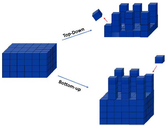
Particularly, in building specific device structures and studying the expected I-V performance. It has been demonstrated, as an example, using a 3DS quantum simulator of Atlas numerical which is built based on non-equilibrium green’s function formalism the physical channel contraction upon nanowires integration with Field Effect Transistors (FET) [8]. The fabrication approaches and progress of growing Si-NWs are based mainly on; bottom-up and top-down techniques. The direct epitaxial growth of Si-NWs from a catalyzing material on a substrate are called bottom-up growth technique. While photoresist patterning on top of a silicon substrate followed by etching to create vertical structures is explained as top-down approach (Figure 1). Where The details of top-down Si-NWs fabrication approach can be found elsewhere [5,13]. The pioneer work in 1965, carried out by Wagner and Ellis [14-16], has led the current work on Si-NWs. The VLS growth system uses metallic droplets or particles (after annealing the sheet layer of metals on the Si substrate), as a seed material nucleating the growth of Si-NWs and adsorb Si gaseous atoms of SiH4 precursors then precipitate to allow crystal growth. The classical example of growing Si-NWs is the VLS system where gold (Au) metal act as a catalyst eutectic droplet. A recent work by Ramanujam, et al. [17] has report-ed the growth and properties of Si-NWs. It has been reviewed various growth methods currently employed in bottom-up Si-NWs growth with special attention on Au and non- Au catalysts. Au is the most widely used catalyst for Si-NWs growth by CVD under VLS mechanism, as it offers a good size control. Indeed, there are other growth mechanisms such as vapour– solid–solid (VSS), Solution–liquid–solid (SLS) at the Ultra High Vacuum Chemical Vapor Deposition (UHVCVD) reactor, or using the advanced Molecular Beam Epitaxy (MBE), or laser ablation which have been employed to address issues related to control Si-NWs, such as, diameter, aspect ratio, position. Moreover, catalyst free ox-ide- assisted methods have also been utilized to grow Si-NWs. Precise positioning of nanowires can be achieved by Electron Beam Lithography (EBL) [18]. Studying the physical properties of the structure of Si-NWs is predominantly critical so that a reproducible relationship between their required functionality and role with their geometrical characteristics can be built. Si-NWs may possess disparate properties due to differences in their crystal phase and directions, crystalline size, i.e., bulk substrates (3D), and nanowires (1D), or thin film or nanomembranes (2D), surface conditions, and aspect ratios.
Most studies to- date have used Au as a catalyst for Si-NWs due to the ease of handling that arises from its high resistance to oxidation [1,4,19]. Indeed, the interest in other metals to seed the growth of Si-NWs has arisen from the fact that Au impurities in Si de-creases the carrier mobility, lifetime, and diffusion length, as Au act as a deep level trap [20]. From the practical point of view, it is desirable to avoid using Au as a catalyst of Si-NWs growth [21]. Based on the previous, the gap in the knowledge of Si-NWs growth and applications is a comprehensive study on Si-NWs catalysed with elements such as Al which assist the growth and alloy for advanced applications. The concept of growing semiconductor nanowires is presented in the next session, along with selected resembling tabulated information of growth techniques and catalysts materials. Where semiconductor nanowires section leads us to a more a specific topic of silicon nanowires and related techniques and applications.
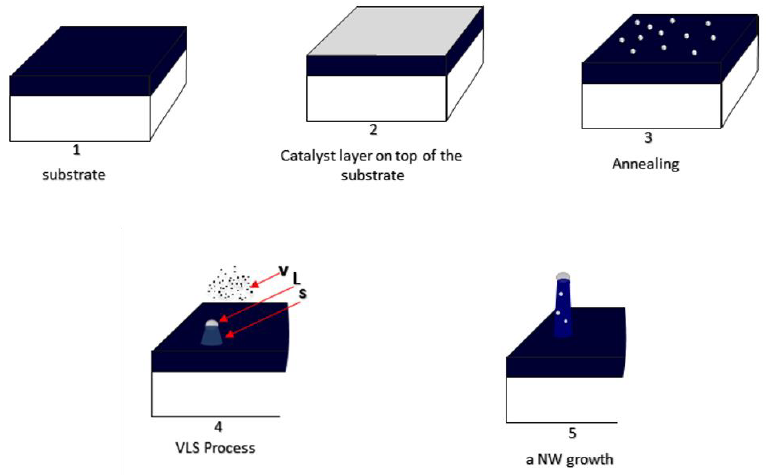
The bottom-up growth of Si-NWs can be described as shown in Figure 2; in the first step depicted in the figure, bulk Si substrate, or a thin grown layer of Si on a cheap substrate such as PC (polycarbonate), PMMA (polymethyl methyl acrylate) or glass. In the second step, a few nanometers thick metal catalyst deposited on the surface, which upon annealing it segregates in isolated droplets in the third step. Precursors gas flows in the Ultra High Vacuum Chemical Vapor Deposition (UHVCVD) reactor such as silane (SiH4), where Si atoms react at the metal-droplet surfaces and dissolve into solution within the metal (step 4). The catalyst materials supersaturate, inducing precipitation of crystalline Si vapor atoms upon the substrate. As precipitation occurs only at the droplet metal (liquid)–semiconductor (solid) interfaces, the semiconductor atoms crystallite in wire structures with diameters controlled mainly by the diameter of the metal droplet (step 5). This growth practice has been termed by Wagner and Ellis as VLS growth after the three co-existing phases: the vaporous precursors (such as Siv), liquid catalyst droplets (such as Aul) and the solid silicon substrate (Sis). Notice the incorporation, which is quite likely, of some of seed metal atoms within the grown Si-NWs, as it has been described schematically in Figure 2.
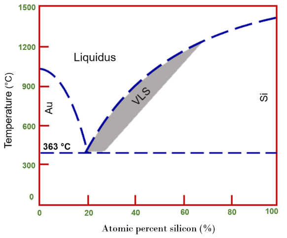
The cutting-edge technology of growing semiconductors for advanced applications is MBE where the control can be down to atomic level. MBE is an ultra-high vacuum technique that is used when thin films of the highest quality and an atomic-level perfection is required. Where Shuji Nakamura, awarded the Nobel Prize in 2014 on the invention of the blue InGaN LED using the MBE system [22]. Moreover, the very recent work by Sadeghi et al. [23]. On growing BaZrS3 chalcogenide perovskite thin films by MBE [22- 24]. The technique of Nanoscale Chemical Templating (NCT) which was invented in 2013 by Khayyat et al, controlling the position of growing Si-NWs using chemically active catalysts [23]. Based on the binary phase diagram, as shown in Figure 3, of Si and Au, the lowest melting temperature for the Au–Si eutectic is 363 °C. The eutectic is lower than the melting points of Au and Si, which are 1064 °C, and 1414 °C respectively [21]. Considering that the liquid phase of the metal is thermodynamically equilibrated with the solid one of the substrate, the lowering of the melting point, with the size of the droplet is given by equation 1 [13];

Where δT is the lowering of the melting point, σ is the interfacial-energy, T0 is the melting point of the bulk metal, ρ is the material density, L is the latent heat, r is the radius of the circle of the catalyst.
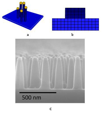
As shown in the phase diagram in Figure 3, the eutectic temperature can be summarized as a mixture of two elements at certain proportions that its melting point is much lower than the melting point of either of the two elements that make it up. Thus, annealing the samples which composed of Au film evaporated on Si substrate to the liquid Au–Si eutectic temperature of 363 °C. If these Au–Si alloy droplets are placed in an ambient containing a gaseous silicon precursor such as silane (SiH4), the precursor molecules decompose into Si and H2 at the outer surface of the metal droplets, thereby supplying additional Si to the Au–Si alloy. It has been confirmed experimentally [1] that Si-NWs grow perpendicularly on Si(111), as it is represented in Figure 4. However, the growth direction of the Si-NWs by any possible variation on one or more growth parameters including the growth temperature, which can be attributed in term of surface/interface energy [1,13,15,16].
There are a number of CVD systems exist, these can be classified by several parameters mainly the base and operation pressure, such as Ultra High Vacuum Chemical Vapor Deposition (UHVCVD) [25,26] . In the VLS wire growth the radius of the seed droplet relates to the radius of the nanowire as described in Equation 2 [15].

Where σl is the surface tension of the liquid catalyst, and σls is the surface tension of the liquid catalyst interface, r is the radius of the Si-NWs, and R is radius of the seed droplet or catalyst. Studying the various related growth parameters of pressure, temperature and position are of critical importance for implementation of Si- NWs as building units at various applications.
Si-NWs for device fabrication. Photo lithography or Electron-Beam Lithography can be used for predefining the precise position of the catalysts, and consequently the spatial placement of nanowires. The topic of controlling the growth position of Si-NWs is an active research topic among several research groups [1,27-36]. Most of the well-established research projects on positioning Si-NWs for further device integration have used Au. The innovative approach of the spatial placement of Si-NWs known as Nanoscale Chemical Templating (NCT) has several advanced applications. NCT main application is growing Si-NWs catalyzed Al, which is p-type dopant and a standard metal in silicon process industrial line. The technique is based on patterning a substrate, such as Si, Ge, or GaAs, which is capable of forming alloys with Al during a following annealing step [26]. The concept of the NCT technique arises as a technical innovative solution of the issue of the defective thin planar grown layer (a few nanometers) between the grown Si-NWs, during the time of growing several hundreds nanometers of NWs Now, what does make NCT an innovative solution? [26]. NCT technique is a method involves the following advantages;
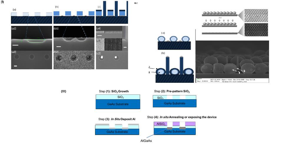
I. Does not require seed material removal (Al) (Figure 5(I)).
II. Does not require any lithography steps (Figure 5(II)).
III. Multiple application space (Figure 5(III)).
I. i.Figure 5(I) explains how NCT does not require Al removal. (I-a) shows the patterned oxidized surface of the Si substrate forming SiO2 layer after photo- or electron beam-lithography. (I-b) shows schematically the sample after Al deposition and annealing, where agglomeration occurs of Al:Si feature in the openings forming the NW seeds, while the Al in contact with SiO2 has reacted with and roughened the surface. (I-c) shows the NW growth. Notice that a single NW per opening is achieved with fidelity higher than 90%. [24] (I-c3), (I-c4) show a larger area containing both a patterned area and an area with no oxide on the left where random growth appears. Silica microsphere can be used to control the position of the grown Si-NWs, as described in 5 (II). In comparison to the previous approach of lithography, here silica microspheres play the role of SiO2 layer in templating the growth placement of Si-NWs. The schematic representation of spinning silica microsphere, where no lithography is required, on Si substrate, followed by a thin layer evaporation of Al (10nm) and the subsequent step of annealing as shown in (a), where (b) shows the Si-NWs growth between silica microspheres, where growth optimization can be undertaken in future work.
The concept of patterning III-V semiconductor materials selectively is of high industrial importance and it is considered as one of the applications of the NCT technique (III) [26]. This suggested application can be extended to forming novel patterning in III-V semiconductors (Figure 5(III)). For example, Al reaction with GaAs will lead to formation of GaAl As selectively in exposed GaAs regions, thereby allowing to obtain patterned GaAlAs and GaAs regions adjacent to each other. Such structures have applications for optoelectronic and FET-like devices (Figure 6).
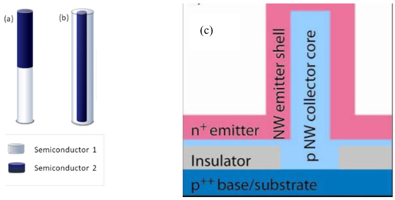
There are several applications of the NCT technique of Si- NWs, such as photovoltaic (PV) made of p-n junctions of NWs as shown in figure 6, or can be used to improve the resolution of Atomic Force Microscopy (AFM) (Figure 7) [27], and in Metal Oxide Semi-conductor Field Effect Transistor (MOSFET) to overcome the technological limit of the channel length using Si-NWs meeting the target of miniaturizing as shown in figure 8
Photovoltaic Cells
PV Cells made of Si-NWs p-n junctions have attracted the attention of the scientific community, because of their potential benefits in their short carrier diffusion length across the diameters of the NWs, and their high light absorption. There are several potential benefits of Si-NWs solar cells over conventional bulk Si one or thin film devices related primarily to cost reduction. This is basically because the Si substrates do not need to be of high purity to fabricate solar cells of Si-NWs. The potential cost of the PV cells reduces by lowering the purity standard and the amount of Si substrates [6]. There are several re-search groups are working in developing PV cells based on Si-NWs. The Lieber [20] and Atwater [12] and other groups [5,37] have developed core-shell growth for their Si-NWs p-n junctions. Moreover, the ability to make single-crystalline Si-NWs on low-cost substrates such as Al foil represents an extra parameter to reduce the overall cost of the cells. Catalysing the growth of Si-NWS and p or n doping the grown Si- NWs at the same time will be of potential importance for advanced applications. Catalysts can be selected based on phase binary phase diagrams [1].
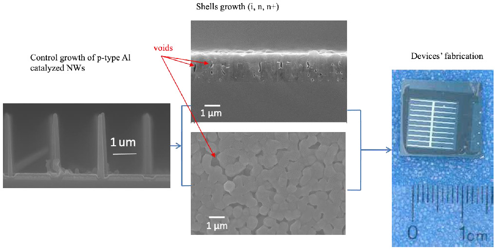
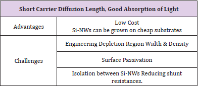
During devices’ characterization it has been noticed that some of the PV Si-NW de-vice are shorted junctions. To study this problem two experiments were designed, to investigate the growth temperature of the capping layers (planner growth without NWs) on Si(100) and Si(111) and measure the shunt resistance vs. position of the grown layer. The shunt resistance varies slightly across the surface of the sample; however, it was low indicating defective planner growth. On the other hand, the growth temperature seems to affect the potential barrier. At this point it was thought that it is important to come up with a method to isolate the planner defective grown areas between NWs from the rest of the device, i.e., nanopatterning. This necessarily eliminates all of the previously described methods of templating the growth, because the metals cannot be protected from oxidation during the patterning processes. The current NCT technique presents a technique that us-es the oxygen sensitivity to template the growth of nanowires with Al and other oxygen reactive materials. In NCT technique, SiO2 layer has been used as a separation layer be-tween the planar defective growth [5,12]. Rectifying junctions of an array of Si-NWs, catalysed by Al, were fabricated (Figure 7). The prepared junctions have exhibited slight light sensitivity, which yield relatively low energy conversion efficiency. However, the fact that silicon solar cells based on nanowires have very short p-n junctions which might increases the carrier collection in the core-shell of the nanowire structure. The above stated details of advantages and challenges of PV devices based on Si-NWs can be summarized as follows (Table 1). The possible advantages of integrating Si-NWs in relatively large scale solar cells make further investigations worth through simulation and experimental studies for future generation devices. The cumulative effort of various research groups, including ours, have worked to point out the technical challenges which of producing large area (>mm2) solar cells from core-shell Si-NWs and other related structures [38]. Rectifying junctions of an array of Si-NWs, catalysed by Al, were fabricated. The shunt regions between the NWs were identified, and a novel oxidation scheme of NCT technique was employed.
Atomic Force Microscopy
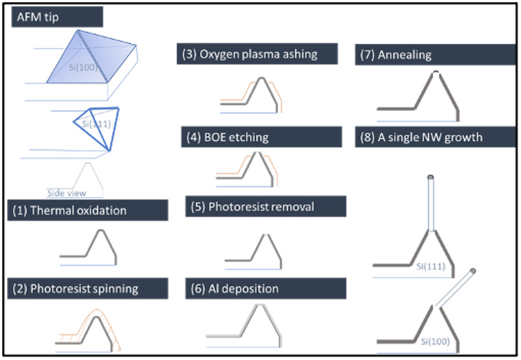
AFM is a machine invented in 1968, for imaging the surface of samples at scales ranging from microns to nanometer, by means of mechanical forces. The AFM consists mainly of three parts: the optical head, the scanner, and the base. The optical head is the main part of the AFM, which is called sometimes the optical sensing system. It is made of a very sharp tip (few nm wide) which is extended down from the end of a small cantilever of SiN or Si (~100μm long), and an optical system to sense the cantilever deflection. The fast progress of nanoscience has been benefited from the invention of the AFM, and this development has been increased by the advancement of AFM based on the progress of Si-NWs growth techniques. It has been proposed to improve the resolution of AFM tips in a production scale [27]. The concept of the technique of improving the resolution of the AFM tips is described in Figure 8, along with the various steps of the Si-NW growth on the tip of the available Si(100) or Si(111) AFM tips. Figure 8 is showing an AFM tip comprising a silicon cantilever, an etched silicon pyramid formed near one end of cantilever, and a Si-NW is extending from the apex of pyramid. An oxide coating covers the pyramid surfaces with the exception of an opening from which silicon wire was grown. The wire is typically grown by the VLS method in a CVD reactor, which uses a catalyst to promote the wires growth. Typical catalysts may include metals such as Al, Au, Ti, with Al being the preferred choice. The growth of Si-NWs has two components; the first component is the longitudinal growth, which is the growth promoted by the catalyst, and defines the wire length, and the second component is the radial growth. This component is reason for the tapered shape of wire. The radial growth is usually undesirable and needs to be minimized. Lower growth temperature can reduce the amount of tapering by increase the ratio of the longitudinal growth rate to the radial growth rate. However, the use of a lower growth temperature has some disadvantages among which are introduction of crystal defects and a lower absolute longitudinal growth rate which render the fabrication process more expensive as throughput is reduced.
The use of an Al catalyst provides a unique advantage for obtaining wires with no tapering, i.e. wires that have a constant cross-sectional shape. The wire comprises of two parts, a core and a shell. When Al is used as a catalyst the core will be doped with Al, form an acceptor level in silicon (Ea-Ev=0.067 eV) and as a result the core will be p-type doped. The shell which forms due to the radial growth remains mostly undoped. A Si etchant such as tetramethylammonium hydroxide (TMAH) or potassium hydroxide (KOH) can now be used to etch electively the undoped shell with respect to the p-doped core. It is showing the wire after the shell was etched.
The grown Si-NW on Si(100) of the squared-base tip is 45° tilted, while Si-NW grow perpendicularly on the tip of the AFM tip of the triangular base of Si(111) [32-39]. Where further reduction of the average wire diameter to the nanometer scale can be done via oxidation or hydrogen annealing [8,22-24,40]. The radius of a Si-NW can be reduced using oxidation sharpening technique. The tip with the grown NW is thermally oxidized at 950 °C for a certain time to oxide the outer-most layer the NW, then etch AlSiOx in HF. This enables steeply rising steps to be imaged without the result showing the shape of the AFM tip. AFM can be used to measure surface roughness, scratching, and indentation. The assembled Si- NW scanning tips are suitable for critical topography investigations comparable with the original scanning tips considering the high aspect-ratio nature of NWs and the superior mechanical hardness [41-43]. Moreover, the growth direction can be tailored based on the required AFM investigations. On Si (111), NWs will grow perpendicularly, where as they grow 45° tilted on Si(100) surfaces.
Metal Oxide Semiconductor Field Effect Transistors
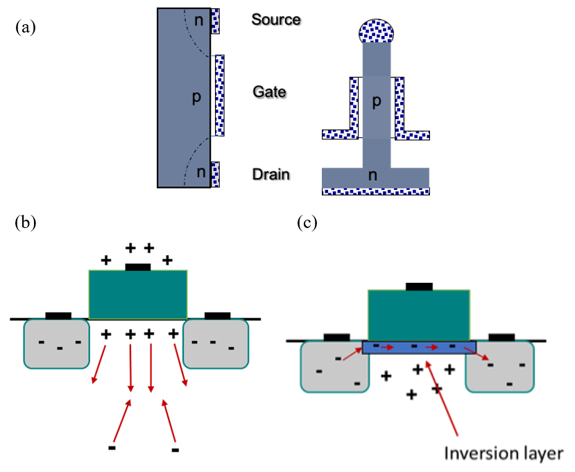
MOSFET current technology can be improved in some of its parts using Si-NWs, as shown in Figure 9 [8]. Employing Si-NWs as a conduction channel of the npn MOSFET between the source and drain for minimizing the short‐channel effects. When a positive voltage is applied to the gate (p-type) the holes in the p-type semiconductor are repelled from the surface (the opposite voltage is correct for pnp MOSFET), then the minority carrier conduction electrons are attracted to the top surface of the transistor. The applied gate voltage exceeds the threshold value, to be followed by an inversion layer formation at the uppermost layer providing a conduction channel between the source and the drain. The width of the conduction channel is controlled by the diameter of the Si- NWs. Where the presented a 3-D schematic diagram of the circular gate-all-around Silicon On Insulator (SOI) nanowire FET with z-axis physical symmetrical contraction, in a structure can be called resonant tunnelling nanowire FET (RT-NWFET). The are more key parameters have showed superior properties, where it can be speculated that, the built device via simulation, of RT-NWFET would be an important device for the complementary MOSFET applications. Moreover, effective integration of Si-NWs and MOSFET will result in modern complementary metal‐oxide‐semiconductor (CMOS) technology along with memory applications. Because of the enhanced surface to volume ratio of NWs, their transport behavior may be adjusted by altering their surface conditions, and this property may be utilized for sensor applications. Si-NWs sensors will potentially be smaller, operate with less power, and react faster [40-42]. The concept can be extended to forming novel patterning in III-V semiconductors. For example, Al reaction with GaAs will lead to formation of GaAl As selectively in exposed GaAs regions, thereby allowing to obtain patterned GaAlAs and GaAs regions adjacent to each other. Such structures have applications for optoelectronic and FET-like devices.
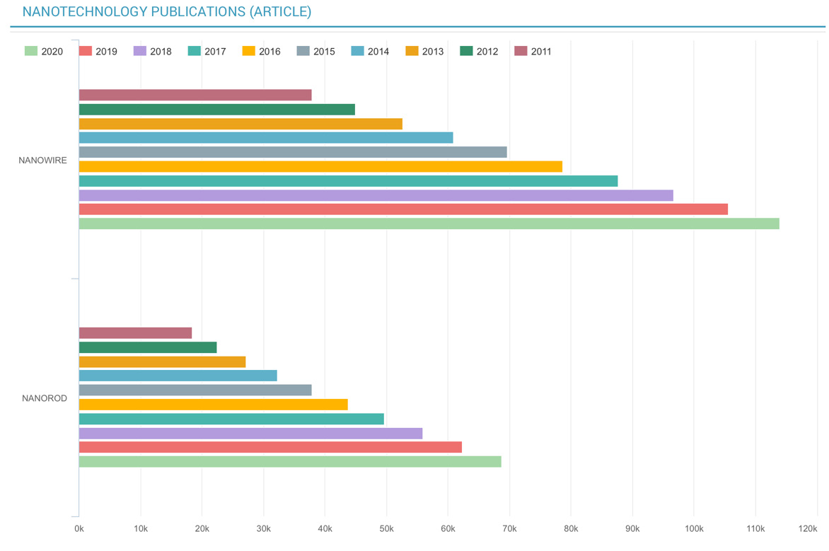
This review is an attempted to shed some lights on the progresses made during the last decade, ranging from Si-NWs growth with control of their position at the nanoscale level [38]. The properties of epitaxial growth of Si-NWs, along with some potential applications of stand-alone Si-NWs or integrated with other well established technologies for further development. We conclude this review article with some remarks for future research, with some direct questions as follows; Will nanowires research provide new windows for new science? Will it guide researchers to new applications? [44-47]. Studies of nanowire and/or nanorods are among the most active topics of nanotechnology, as shown in figure 10, where the total cumulative published studies starting from 2011 up to 2020 have been increased quite markedly exhibiting the technological importance of this research area. The scientific community tend to describe the 1D structures as nanowires or nanorods. If there is any technical difference between nanowires and nanorods them is assigned to the relative ratio between their diameters to their lengths. This ratio is smaller in case of nanowires. Scientists sometimes use nanowires and nanorods equally. Nanowires are one dimensional nano-structures which have diameters of the order of tens of nanometers, with unconstrained length scales. The ratio between their diameters to their lengths may be less than 10-3. While for the nanorods, that ratio here is almost ranged between 0.1 and 0.3 only (Figure 10).
Nanomaterials like the nanowires or nanorods have dimensions within the nanometer range. They are called one- dimensional nanostructures materials. The difference between them and their naming are attributed to the relative ratio between their lengths to their diameters, i.e.; their aspect ratios. The aspect ratio is smaller in case of nanorods, it could be in the range of 3 to 5. While nanowires have diameters of the order of tens of nanometers, with unconstrained length scales, with aspects ratios could be above 1000. The ever-growing demand for smaller electronic devices is prompting the scientific community to produce circuits whose components satisfies size and weight requirements. This demand can be reached be employing Si-NWs, considering their distinct properties, and their combined attributes of cost effectiveness and mature manufacturing infrastructures and use them as nanocomponents to build nano circuits and nano biosensors. [43- 46]. Control of the synthesis and the surface properties of Si-NWs may open new opportunities in the field of silicon nanoelectronics Moreover, To sum up, semiconductors will continue to inspire us and improving our life quality via continuous dedicative research activities, overcoming the current fabrication barriers [46-51]. MOSFET is the key unit of electronic industries, microprocessors, memory chip, and telecommunications circuits. Based on this, any possible limitations with MOSFET technologies, will consequently affect the other related applications [52,53]. Moore observed an exponential doubling in the number of transistors in every 18 months through the size reduction of transistor components. This limitation is directly related to the fact that we cannot break down the atomic size barrier, which implies a fundamental size limit at the atomic/nucleus scale. After all, there is no more direct 18-month doubling, instead there are other forms of transistor doubling may happen at a different slope, which opens doors for more research on nanowires and other nanotechnological unit integration [8]. Simulation models of suggested device structures can provide foresight report of the possible approaches of the various available nanostructure integrations [54-61].